This article was last revised in 183 Days ago, some of its contents may have changed. If you have any questions, you can ask the author。
Scanning Electron Microscopy (SEM) is a microscopy technique that uses a focused electron beam to create detailed images of the surface of a sample. The electron beam scans the sample in a raster pattern, and the resulting signals generated by interactions between the electron beam and the sample's surface are detected and used to form an image. SEM provides high-resolution three-dimensional surface images and is widely used in various fields, including material characterization, nanotechnology, and biological research.
Energy-Dispersive X-ray Spectroscopy (EDS): EDS is an analytical technique often used with SEM. It detects characteristic X-rays emitted by a sample when it is bombarded with an electron beam. The energy and intensity of these X-rays provide information about the elemental composition of the sample. SEM EDS allows the identification and quantification of elements present in the sample, offering valuable insights into its elemental makeup and chemical characterization.
Energy-Dispersive X-ray Analysis (EDX): EDX is another term for EDS and refers to the analysis and investigation of samples using energy-dispersive X-ray spectroscopy. It involves the detection and analysis of X-rays emitted from a sample, which carries information about the elements present and their concentrations. SEM EDX is a powerful tool for qualitative and quantitative elemental analysis, identifying trace elements, and mapping elemental distribution across a sample.
The combination of SEM and EDS/EDX offers several advantages and applications:
1. Elemental Analysis
SEM EDS/EDX allows for qualitative and quantitative elemental analysis of samples. It can identify the chemical composition and elemental distribution within a material, including trace elements.
2. Material Characterization
This technique is widely used for characterizing various materials, such as metals, minerals, polymers, ceramics, and biological samples. It helps determine the elemental composition, the presence of impurities, and the identification of phases or compounds within a sample.
3. Failure Analysis
SEM EDS/EDX is valuable in investigating material-related failures and defects. It can identify the causes of failures by analyzing the elemental composition and identifying foreign particles or contaminants.
4. Geological Analysis
SEM EDS/EDX is extensively utilized in geology to study the composition and structure of rocks, minerals, and soil. It aids in the identification of minerals, the study of rock textures, and the analysis of geological processes.
5. Forensic Science
SEM EDS/EDX plays a crucial role in forensic investigations, assisting in the analysis of trace evidence, such as fibers, gunshot residue, paint chips, and glass fragments. It can help identify and compare materials found at a crime scene.
Overall, EDS/EDX in SEM is a powerful analytical tool that combines imaging and elemental analysis. It finds applications in various fields, including materials science, geology, forensic science, environmental analysis, biology, and archaeology.
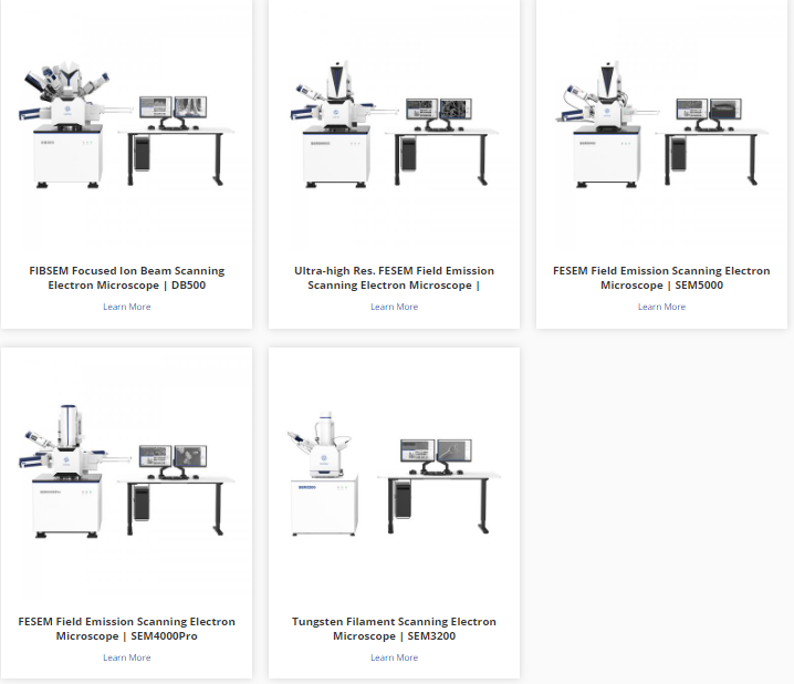
CIQTEK's self-developed SEM Microscopes offer a wide range of electron detectors, such as BSED, STEM, EDS, EDX, EBSD, In-lens, ETD, etc.
