- What is SMD Packaging Technology?
- The Core of SMD Packaging Technology
- Advantages of SMD Packaging Technology
- Applications of SMD Packaging Technology
In the LED display industry, performance and image quality improvements often hinge on small but crucial technological advancements. Among them, SMD packaging technology (Surface Mount Device) is undoubtedly a driving force in the evolution of LED displays. But what exactly is SMD packaging, and how does it impact LED displays? Let’s explore.

- What is SMD Packaging Technology?
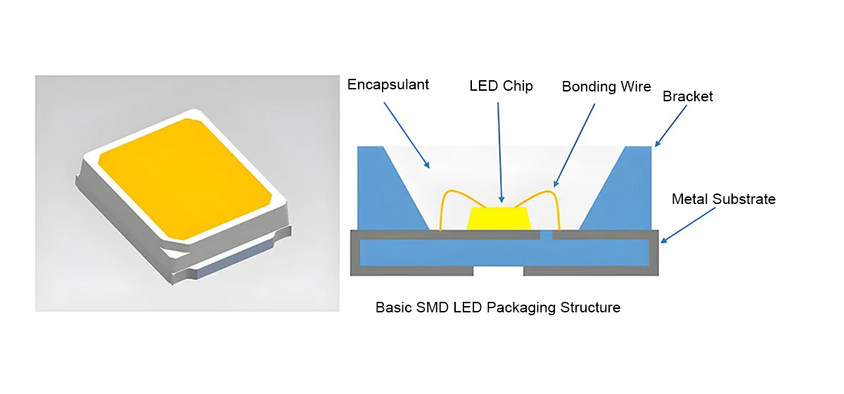
SMD packaging, short for Surface Mounted Device, involves encapsulating LED chips, supports, and bonding wires into compact, lead-free LED beads, which are then surface-mounted onto printed circuit boards (PCBs) using automated machines. Compared to traditional DIP (Dual In-Line Package) technology, SMD offers higher integration, smaller size, and lighter weight, driving miniaturization and efficient production of LED displays.

- The Core of SMD Packaging Technology
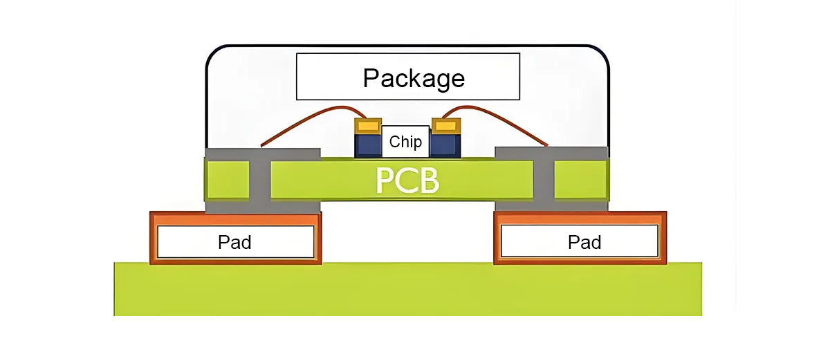
At its core, SMD packaging mounts the LED chip directly onto the surface of the circuit board rather than inserting it through traditional holes. This surface-mount approach enables the miniaturization of components, improves production efficiency, and facilitates automation.

- Advantages of SMD Packaging Technology
High Integration and Miniaturization
SMD technology allows LED components to be compact and lightweight, ideal for high-density integration. This results in smaller pixel pitch and higher resolution, enhancing image sharpness and clarity.
Efficient Production
Automated pick-and-place machines significantly boost production efficiency. Compared to traditional manual soldering, SMD technology speeds up the mounting of numerous LED components, reducing labor costs and shortening production time.
Excellent Heat Dissipation
SMD-packaged LED components are in direct contact with the PCB, facilitating heat dissipation. Effective thermal management extends the lifespan of LEDs and enhances the stability and reliability of the display.
Easy Maintenance and Replacement
Since SMD components are surface-mounted on the PCB, they are easier to repair and replace, lowering maintenance costs and downtime.
Cost-Effective
Automated production reduces manufacturing costs, making the products more affordable.
- Applications of SMD Packaging Technology
LED display models using SMD packaging technology are widely applied in various scenarios, including small-pitch LED displays (P1.2, P1.5), indoor displays (P2, P2.5), outdoor displays (P4-P10), as well as transparent and flexible screens. SMD technology provides these models with high resolution, wide viewing angles, strong weather resistance, and energy efficiency, making them ideal for advertising, conferences, stages, and sports venues.

SMD packaging technology is one of the key driving forces behind the advancement of the LED display industry. Its high integration, automated production benefits, and superior heat dissipation have enhanced the overall performance of LED displays, providing higher resolution, wider viewing angles, and strong weather resistance, suitable for various indoor and outdoor applications. As technological innovations continue, SMD packaging will remain a vital player in the evolution of LED display technology.